

On May 9, 2025, First Solar, Inc. (“First Solar”) filed a lawsuit against Canadian Solar Inc. and its affiliates (collectively “Canadian Solar”), alleging infringement U.S. Patent No. 9,130,074 (“the ’074 patent”). First Solar, Inc. v. Canadian Solar Inc., Case No. 1:25-cv-00582, Dkt. No. 1 (D. Del. May 9, 2025).
The complaint alleges that plaintiff First Solar is “the only U.S.-headquartered company among the world’s ten largest producers of solar products,” First Solar, Dkt. No. 1, ¶2, and “owns a large portfolio of patents. . . including patents on TOPCon technology,” id. at ¶6. The complaint describes the ’074 patent as “one of First Solar’s TOPCon patents.” Id.
The complaint further alleges that Canadian Solar, a photovoltaics company that has historically manufactured its products in China, has engaged in unfair competition with American companies by dumping solar modules on the U.S. market. First Solar, Dkt. No. 1, ¶7
On August 22, 2025, Canadian Solar (USA) Inc. petitioned for inter partes review of the ’074 patent. Canadian Solar (USA) Inc. v. First Solar, Inc., IPR2025-01130, Paper 1 (PTAB Aug. 22, 2025).
The ’074 patent, titled “High-Efficiency Solar Cell Structures and Methods of Manufacture,” describes a solar cell structure having “[m]ultifunctional layers [that] provide combined functions of passivation, transparency, sufficient conductivity for vertical carrier flow, the junction, and/or varying degrees of anti-reflectivity.” The ’074 patent, 1:46-54.
According to the patent and as shown in the figure below, an exemplary cell includes front and back metal electrodes 81, 89, an antireflection film 82 on the front side, a transparent and conductive film 88 on the back side, electrically passivating and conductive film layers 83, 86 and electrically passivating interface layers 84, 86 sandwiching an n-type crystalline silicon wafer 85. The ’076 patent, 6:36-7:34.
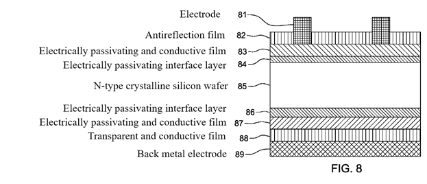
The ’074 patent, Fig. 8 (annotated).
The ’074 patent describes the electrically passivating interface layers 84, 86 as being less than 10 nm thick, with no conductivity requirements or absorption restrictions due to their “small thickness.” The ’074 patent, 6:65-7:4; id. at 7:8-13.
The ’074 patent describes the electrically passivating and conductive film 83 as “highly n-doped,” and the electrically passivating and conductive film 87 as “highly doped p-doped.” According to the patent, both films 83, 87 are made of exemplary materials such as amorphous or polycrystalline silicon carbides, amorphous or polycrystalline silicon, or amorphous or poly-crystalline diamond-like-carbon. The ’074 patent, 6:51-64; id. at 7:14-26.
The ’074 patent also outlines exemplary fabrication methods including: (1) processing the wafer to deposit or grow the electrically passivating interface layers, (2) deposit the electrically passivating and conductive film layers, (3) thermal treatment, (4) deposition of the antireflection film and transparent and conductive film layers, and (5) metallization. The ’074 patent, 15:9-36.
According to the ’074 patent, “good passivation of [electrically passivating interface] layers xx4 and xx6 persists and/or improves after high temperature thermal treatment.” Id. at 16:21-23. The ’074 patent also describes using oxide-containing electrically passivating and conductive films to replace the electrically passivating interface layers:
If the layer composition is chosen correctly, a layer deposited in a single process can split into two (or more) layers. The incorporated oxygen in the amorphous deposited layer migrates toward the silicon interface and a thin oxide can be grown. If this mechanism is exploited by the use of oxide containing [electrically passivating and conductive] films XX3 and XX7, the [electrically] passivating interface layers XX4 and XX6 do not need to be produced prior to layers XX3 and XX7, therefore all described structures can also work without layers XX4 and XX6.
The ’074 patent, 16:38-46.
Claim 1 of the ’074 patent recites:
A method of fabricating a solar cell, comprising;
providing a wafer as a central substrate;
depositing or growing at least one amorphous interface passivation layer over the substrate;
depositing at least one conductive and passivating layer on the at least one interface passivation layer, the at least one conductive and passivating layer comprising a dopant;
providing thermal treatment at a temperature of about 500° C. or higher, the thermal treatment crystallizing, at least in part, the at least one conductive and passivating layer and facilitating diffusion of the dopant from the at least one conductive and passivating layer through the at least one interface passivation layer; and
providing metallization as electrodes which directly contact the at least one conductive and passivating layer following the thermal treatment thereof, wherein the dopant diffused through the at least one interface passivation layer provides shortened charge carrier flow paths between the substrate and the electrodes through the at least one conductive and passivating layer and the at least one interface passivation layer.
The ’074 patent, 19:14-35.
First Solar identifies as Infringing Products “Canadian Solar’s TOPCon solar modules,” including the TOPBiHiKu and TOPHiKu lines. First Solar, Dkt. No. 1, ¶61.

First Solar, Dkt. No. 1, ¶62.
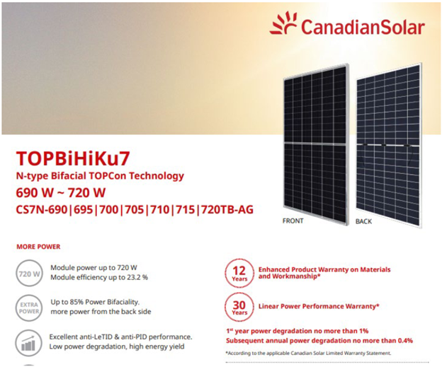
First Solar, Dkt. No. 1, ¶62.
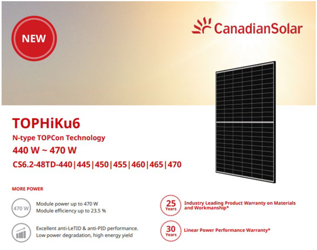
First Solar, Dkt. No. 1, ¶62.
The complaint alleges that “Canadian Solar provides webinars that provide a technological overview of the Canadian Solar TOPCon products and the TOPCon cells used therein,” including an illustration of the structure used in Canadian Solar’s TOPCon products. First Solar, Dkt. No. 1, ¶63-64. The illustration, First Solar alleges, “show[s] layers corresponding to those formed according to method of Claim 1 [of the ’074 patent].” First Solar, Dkt. No. 1, ¶72.
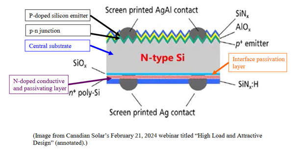
First Solar, Dkt. No. 1, ¶72.
First Solar also alleges that Canadian Solar applies a thermal treatment of at least a temperature of about 500 °C, which crystallizes the n+ poly-Si layer and facilitates diffusion of the dopant phosphorus from the “n+ poly-Si” layer to the SiOx layer. First Solar, Dkt. No. 1, ¶76-77.
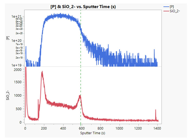
First Solar, Dkt. No. 1, ¶77 (allegedly illustrating phosphorus diffusion relative to the distance from the back surface of a tested Canadian Solar TOPCon cell).
Based on the figure above, First Solar alleges that “[t]he degree of diffusion shown by these data necessarily requires a thermal treatment of the silicon cell assembly at a temperature above 500 °C.” First Solar, Dkt. No. 1, ¶78.